If you wish to make an apple pie from scratch, you must first invent the universe.
The famous quote from Carl Sagan could also be applied to computer science, if you want to make a program from scratch you must first invent the universe. Since I only had 2 weeks vacation, and inventing a whole universe would have been to much work, I skipped a few parts and started with designing a RISC-V core.
The goal wasn’t so much to end up with a usable RISC-V core, but to learn more VHDL, after my initial Merry x-Mas try out. So I started working on a classic 5-Stage pipelined RISC-V core, and that’s when the learning experience begun.
When trying to implement the IF (Instruction Fetch) stage I ran into problems, because I wanted to use the Xilinx BRAM as memory. But BRAM has a 1 (or 2) clock delay, before that data is available on the output. So my 5 stage pipeline design turned into a 7 stage pipeline design, with IF1, IF1, ID, EX, ME1, ME2, and WB.
The next problem was that the pipeline design is a Harvard architecture, so the IF stage and ME stage would want to access RAM at the same time. To do that there must be some arbiter, but here I cheated a bit, and used the BRAM dual port feature. So instructions are read from port A and data is read and written to port B, which kind of makes the BRAM its own arbiter.
To get a bit of an overview, I quickly setup VHDL entities for all 7 pipeline stages and started to implement and connect them with Vivado.
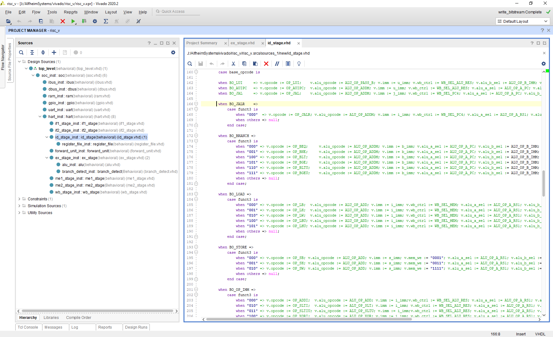
That of course turned into one big mess, so I started to combine signals into groups. For example I combined all registered signals that go from the IF2 to the ID stage in a if2_to_id_buf_type record as follows;
type if2_to_id_buf_type is record
    pc      : std_logic_vector(31 downto 0);
    pc4     : std_logic_vector(31 downto 0);
    instr   : std_logic_vector(31 downto 0);
    nop     : std_logic;
end record;
This way the code that connects the IF2 and ID stage only has to use one signal and not 4 (pc, pc4, instr and nop). This change made my code a lot less verbose and easier to read and change;
entity if2_stage is
    port (
        if1_to_if2_buf_i    : in if1_to_if2_buf_type;

        if2_to_id_buf_o     : out if2_to_id_buf_type;

        flush_i             : in  std_logic;
        stall_i             : in  std_logic;

        ibus_dat_i          : in  std_logic_vector(31 downto 0);
        ibus_stall_i        : in  std_logic;

        clk_i               : in  std_logic;
        rst_i               : in  std_logic
    );
end if2_stage;

architecture behavioral of if2_stage is
    signal if2_to_id_buf        : if2_to_id_buf_type;
    signal next_if2_to_id_buf   : if2_to_id_buf_type;
begin
    process(clk_i, rst_i, next_if2_to_id_buf)
    begin
        if (rising_edge(clk_i)) then
            if (rst_i = '1') then
                if2_to_id_buf <= reset_if2_to_id_buf;
            else
                if2_to_id_buf <= next_if2_to_id_buf;
            end if;
        end if;
    end process;

    process(if2_to_id_buf, if1_to_if2_buf_i, ibus_dat_i, ibus_stall_i, flush_i)
        variable v : if2_to_id_buf_type;
    begin
        v := if2_to_id_buf;

        v.pc := if1_to_if2_buf_i.pc;
        v.pc4 := if1_to_if2_buf_i.pc4;
        if (flush_i = '1' or if1_to_if2_buf_i.nop = '1' or ibus_stall_i = '1') then
            v.instr := NOP_INSTR;
            v.nop := '1';
        else
            v.instr := ibus_dat_i;
            v.nop := '0';
        end if;

        next_if2_to_id_buf <= v;
    end process;

    if2_to_id_buf_o <= if2_to_id_buf;

end behavioral;
The line if2_to_id_buf <= reset_if2_to_id_buf; in the code uses the constant reset_if2_to_id_buf to reset the signals, the constant is defined in a library like this;
constant NOP_INSTR : std_logic_vector(31 downto 0) := X"00000013";

constant reset_if2_to_id_buf : if2_to_id_buf_type := (
    (others => '-'),    -- pc
    (others => '-'),    -- pc4
    NOP_INSTR,          -- instr / nop instr
    '1'                 -- nop
);
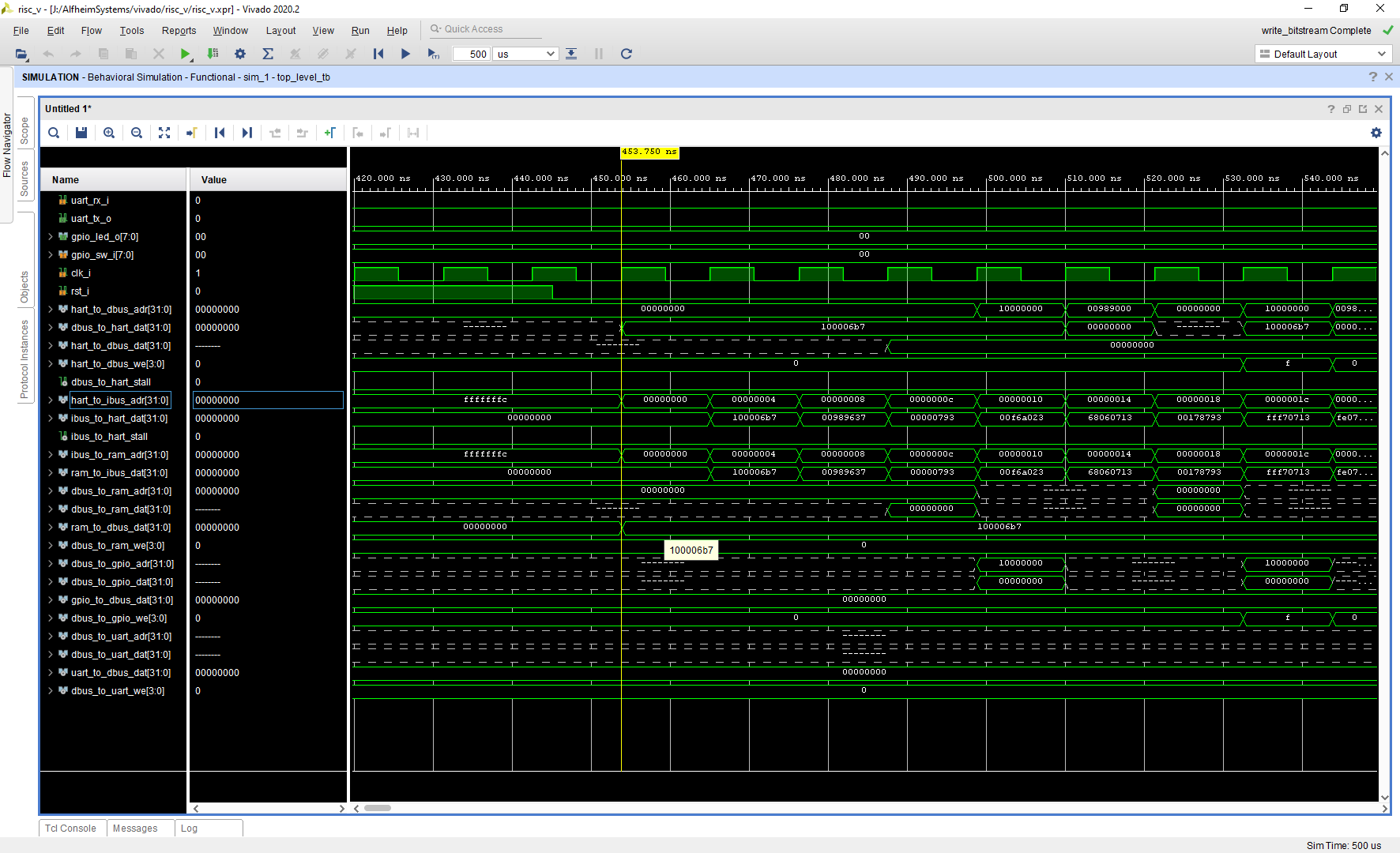
So after implementing all 7 stages like that, it was time to do some testing with Vivado’s simulator.
But before things could be simulated I needed a test program. So I wrote a small assembly program;
  li      a3,0x10000000
  lui     a2,0x989
  li      a5,0
l1:
  sw      a5,0(a3)
  addi    a4,a2,1664
  addi    a5,a5,1
l2:
  addi    a4,a4,-1
  bnez    a4,l2
  j       l1
that endlessly counted up a 32 bit register and wrote the lower byte to the 8 LED’s of the Digilent Nexys Video board. To be able to interact with the outside world I added GPIO and UART (didn’t have time to implement that) address ranges to the dbus so 0x0000XXXX would be RAM, 0x1000XXXX would be GPIO, and 0x2000XXXX would be the UART. This very simple IO system was enough to test the RISC-V core, but in the future it should be replaced with an icache and dcache that than connect to an AXI-master interface so Vivado can connect the core to all other AXI IP blocks it has, but that was way to much work for the 2 week time frame I set myself.
The next problem was how do I get the program in the RAM, and here I went for the quick and dirty solution, I simply copy and pasted it into the BRAM init code like this;
      INIT_00 => X"fe071ee3fff70713001787936806071300f6a0230000079300989637100006b7",
      INIT_01 => X"00000000000000000000000000000000000000000000000000000000fedff06f",
It ain’t pretty, but it works, and it is still faster than punching and patching punched cards to program a computer :-)
So now the real testing could start, and of course things failed miserably. The biggest problem was that I didn’t implement hazard detection. So when an instruction changes a register value, and the next instruction needs the result it isn’t there yet, because the result only made it to the ME1 stage of the pipeline and would need 3 more clock ticks to reach the register file. To fix this in a quick and dirty way I added nop instructions all over the program;
  li      a3,0x10000000
  lui     a2,0x989
  li      a5,0
  nop
  nop
  nop
l1:
  sw      a5,0(a3)
  nop
  nop
  nop
  addi    a4,a2,1664
  nop
  nop
  nop
  addi    a5,a5,1
  nop
  nop
  nop
l2:
  addi    a4,a4,-1
  nop
  nop
  nop
  bnez    a4,l2
  nop
  nop
  nop
  j       l1
That kind of worked except for the jump and branch instructions, so I implemented a forwarding unit that forwarded the register values of the ME1, ME2, and WB stage to the EX stage so there didn’t need to be any nop instructions in code stream. I also added a flush for the jump and branch instructions.
Of course there is no such thing as a free lunch, because of the added logic the path from the BRAM became to long and I needed to reduce the speed from 100MHz to about 80MHz.This could be fixed by adding an extra IM3 stage to the IM1, and IM2 stages, so the output of the BRAM can be registered, and so the logic path is divided into two shorter paths. Of course adding extra pipeline stages can mean throwing away more work in case a flush is needed, no free lunch.
Now things looked OK in the simulator and the clock speed was lowered enough to actually implement it in the real FPGA, the big moment was there, programming it and see what happens;
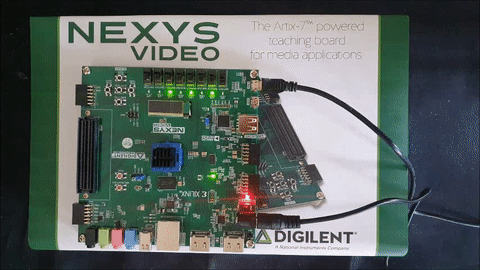
2 weeks of work, 400 Euro of hardware, and we have some blinking LED’s !
So is this a working and usable RISC-V core? The short answer is, no. The bit longer answer is, maybe. The list of things that are missing is long;
- no irq/exception support
- no mul/div support
- no external bus like AXI
- no test benches for the sub parts like ALU
- no way to load programs other than hard coding them in BRAM
- etc. etc.
But I think it has potential, and I will certainly work on it in the future, especially since I learned a lot the last 2 weeks.
For everybody that wants to take a closer look, the source code is available on github